
Next-Generation Micro LED Manufacturing in China: Technological Roadmap & OEM Sourcing Guide
The global spatial computing, augmented reality (AR), and automotive Head-Up Display (HUD) markets are experiencing a monumental paradigm shift. As legacy liquid crystal displays (LCD) and digital micromirror devices (DMD) hit physical limits in luminance, power efficiency, and form factor density, Micro LED (Microscopic Light Emitting Diode) technology has emerged as the definitive display architecture for next-generation optoelectronic systems.
As China’s leading industrial Micro LED manufacturer and display engine foundry, our semiconductor facility bridges the gap between high-yield epitaxy growth, wafer-level mass transfer, and final optical engine assembly. Operating state-of-the-art Class 10/100 cleanrooms and advanced CMOS backplane hybridization lines, we deliver monolithic full-color Micro LED arrays and high-brightness optical engines tailored for global tier-1 defense contractors, medical device manufacturers, consumer electronics brands, and automotive OEMs.
This comprehensive technical whitepaper details the architectural superiority of semiconductor-grade Micro LEDs, outlines global procurement trends, provides comparative engineering benchmarks, and explains how enterprise buyers can de-risk their micro-display supply chain through strategic sourcing in China.
Micro LED vs. Micro OLED vs. LCoS: Quantitative Display Performance Benchmarks
When engineering high-ambient visibility optical systems—such as outdoor AR smart glasses, fighter jet helmet visors, or automotive transparent HUDs—display selection directly dictates battery longevity, thermal dissipation budget, and optical waveguide efficiency.
| Performance Parameter | Monolithic Micro LED (InGaN/AlGaInP) | Micro OLED (Silicon-Based OLED) | LCoS (Liquid Crystal on Silicon) |
|---|---|---|---|
| Peak Luminance (Green / Full-Color) | Up to 3,000,000 nits (Green) / 100k+ nits (RGB) | 1,000 - 5,000 nits | 10,000 - 30,000 nits (Requires external light source) |
| Pixel Pitch / Pixel Density (PPI) | < 3.5 µm (> 7,000 PPI) | 5.0 - 9.0 µm (approx. 3,000 - 4,000 PPI) | 4.5 - 8.0 µm |
| Power Consumption Efficiency | Ultra-High (> 15% EQE) | Moderate (High power at elevated drive currents) | Low (High power due to continuous backlight illumination) |
| Operating Temperature Range | -40°C to +105°C (Extreme Defense Standard) | -20°C to +70°C (Organic material degradation) | -10°C to +60°C (Liquid crystal response slows down) |
| Response Time | < 1 Nanosecond (Sub-microsecond) | < 0.1 Millisecond | 2.0 - 5.0 Milliseconds |
| Contrast Ratio | 1,000,000 : 1 (Infinite Dark Pixel Off) | 100,000 : 1 | 1,000 : 1 (Light leakage on black pixels) |
| Form Factor & Optical Integration | Ultra-compact optical engines (< 0.5cc volume) | Compact, but limited by thermal caps | Bulky (Requires polarizers and beamsplitters) |
Key Technology Trends Reshaping the Micro LED & Spatial Display Sector
As micro-display technology transitions from laboratory prototyping to mass industrial production, several groundbreaking innovations are defining the competitive landscape for 2025 and beyond:
1. Monolithic RGB Integration & Quantum Dot (QD) Conversion
Traditional mass transfer methods involved placing discrete Red, Green, and Blue sub-pixels individually, creating manufacturing bottlenecks. China’s top foundries now utilize native monolithic GaN-on-Silicon growth combined with high-resolution ink-jet printed Quantum Dot (QD) color conversion arrays, achieving sub-3.5µm RGB pixel structures at significantly reduced manufacturing costs.
2. High-Throughput Wafer-Level Mass Transfer (>10M Chips/Hour)
Overcoming the "mass transfer barrier" has been the Holy Grail of Micro LED commercialization. Our facility deploys multi-beam laser-assisted transfer (LIFT) and elastomer stamp technology capable of transferring over 10 million micro-chips per hour with spatial alignment tolerances under 0.5 microns, yielding 99.999% functional die rates.
3. Ultra-Compact Waveguide Optical Engine Coupling
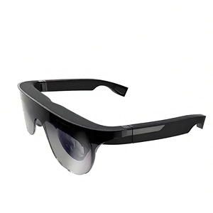
Micro LED light engines are now engineered to directly pair with surface surface-relief grating (SRG) and holographic optical waveguides. By achieving outdoor-readable brightness levels surpassing 3 million nits at the display face, optical efficiency loss inside diffractive waveguides (often 90–95% loss) is comfortably negated, enabling lightweight (under 35g) consumer AR frames.
Strategic Sourcing Trends for Enterprise Procurement & Supply Chain Leaders
Global original equipment manufacturers (OEMs) and system integrators face escalating complexity when procuring optoelectronic hardware. Analyzing global supply chain realignments reveals clear procurement trends shaping enterprise decision-making:
Shift to One-Stop Modular Co-Development (ODM)
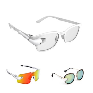
Procurement managers are stepping away from sourcing displays, micro-controllers, optics, and housing components from fragmented suppliers. Leading enterprises now partner directly with integrated China foundries capable of delivering fully aligned optical-display modules—combining Micro LED/Micro OLED panels, custom driver ICs, transparent nylon frame chassis, and anti-fog protective visors under a single unified warranty.
Cost-Scaling Curve Acceleration
Driven by massive 8-inch GaN-on-Silicon wafer manufacturing investments across China's semiconductor hubs, Micro LED micro-display module unit costs are projected to decrease by 45% over the next 24 months. Sourcing partners establishing early long-term supply agreements (LTSA) lock in strategic cost advantages over competitors reliant on legacy Micro OLED or projection optics.
Custom CMOS Backplane Driver Integration
To support high-frame-rate spatial computing (120Hz+) without thermal throttling, procurement specs now demand custom-designed active-matrix CMOS backplanes featuring MIPI, SPI, and low-power LVDS interfaces directly bonded to the micro-display chip via micro-bump bonding.
Why Partner with Our China Micro LED Manufacturing Center?
Building on deep industrial heritage in spatial computing, optical engineering, and rugged tactical equipment packaging, our factory provides a vertically integrated manufacturing pipeline built for international export excellence.
- Semiconductor-Grade Epitaxy & Cleanroom Facilities: Certified ISO 14644-1 Class 10/100 dust-free cleanroom manufacturing ensuring absolute defect control during wafer bonding and mass transfer.
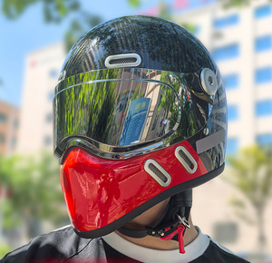
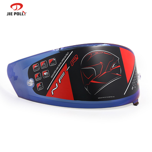
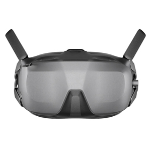
- Full System Integration Capabilities: From micro-display wafer fabrication to custom transparent nylon frame structures, impact-resistant carbon fiber helmet visors, and FPV wide-angle optical systems.
- Rigorous Automated Optical Inspection (AOI): 100% pixel-level luminance uniformity and color consistency testing using ultra-high-resolution scientific CCD camera systems.
- Proven Global Compliance & Quality Management: ISO 9001, ISO 14001, IATF 16949 automotive certified, CE, FCC, RoHS, and 3C & DOT impact-resistant optical compliance.
- Global Service & Logistics Infrastructure: Rapid turnaround prototyping, dedicated bilingual FAE (Field Application Engineering) support, and secure worldwide shipping to over 45 countries.
Micro LED Sourcing & Manufacturing FAQ
Answers to critical questions asked by optical engineers, procurement officers, and enterprise buyers during technical evaluation and supplier auditing.
Accelerate Your Next-Gen Display Project Today
Whether you require custom monolithic Micro LED chips, Micro OLED modules, high-grade transparent nylon frame components, or rugged HUD helmet integration, our engineering team is ready to deliver.
Send an Inquiry